
SEMICONDUCTORControlled Environment Technologies
Industry
Semiconductor
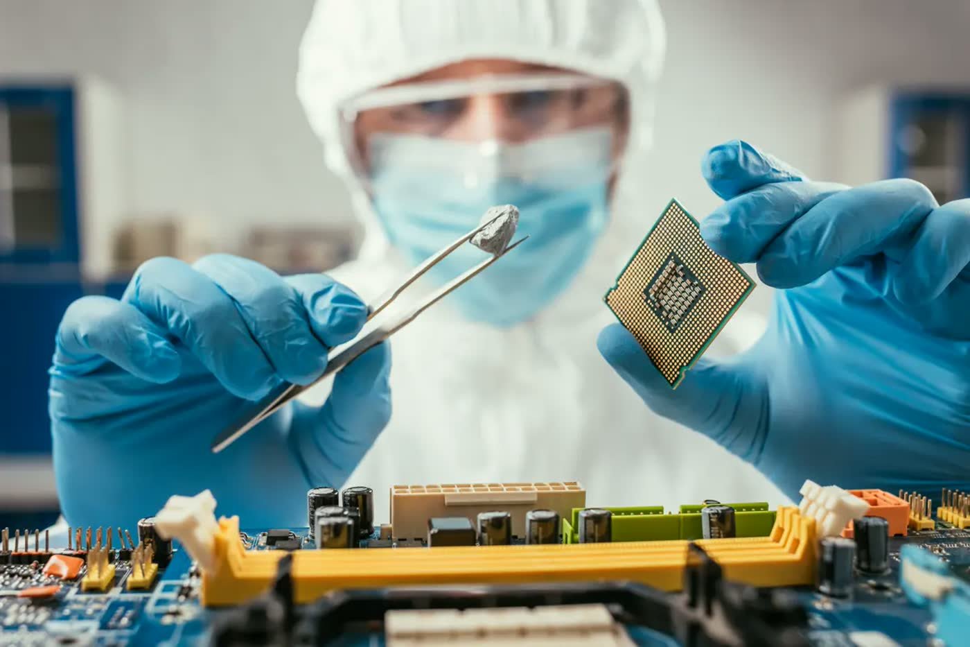
Particle, molecular contamination and electrostatic discharge control in semiconductor manufacturing.
Datasheet per part number
Standards referenced
Recurring consumption
In a fab, the defect that kills a chip is a fraction of the geometry being printed. That is why contamination control in semiconductor work resembles no other industry: clean air is not enough, you also have to control what comes off surfaces, gloves and the very wiper used to clean.
Products for this industry
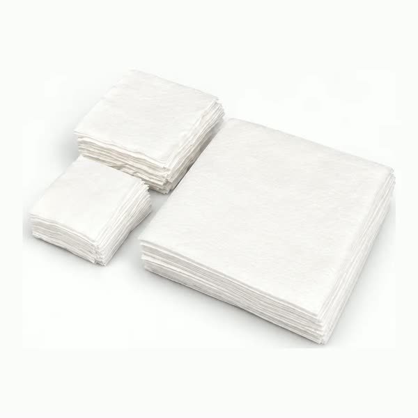
VANTERIS Polyester Wipe 9 × 9 inVTN-WP-PES-LS-999 × 9 in (228.6 × 228.6 mm)

VANTERIS Sticky Mat 24 × 36 in, BlueVTN-MAT-PE-STK-2436-BLU24 × 36 in
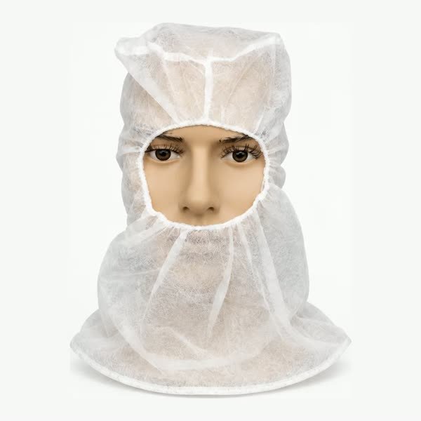
VANTERIS Nonwoven Hood 40 × 42 cm, WhiteVTN-AP-PP-NH-UNI-WHT40 × 42 cm
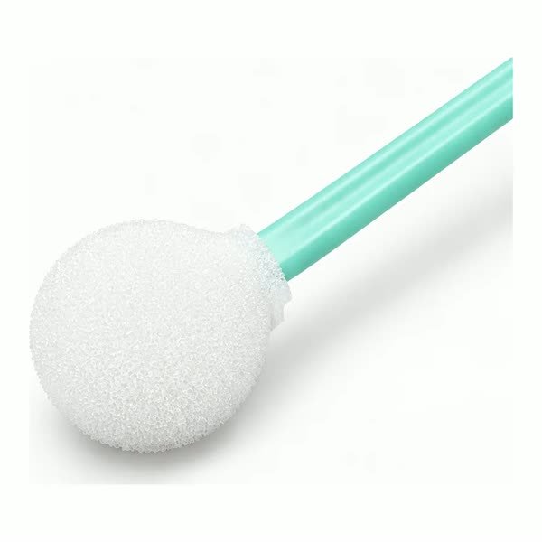
VANTERIS Foam Swab Large Round HeadVTN-SW-PU-LC-132132.2 mm
Typical challenges
- Particles below process geometry
- Molecular contamination in photolithography
- Electrostatic discharge on wafer and device
- Consumable compatibility with process solvents
Reference standards
| ISO 14644-1 | Classifies air cleanliness by particle concentration (ISO Class 1 to 9). |
|---|---|
| ISO 14644-9 | Classifies surface cleanliness by particle concentration. |
| IEST-RP-CC004 | Method for evaluating cleanroom wiping materials. |
| ANSI/ESD S20.20 | Requirements for an electrostatic discharge control programme. |